How to Avoid Getting Totally Skewed, Part 4
When sourcing materials, consider dual-ply glass.
Au: This column is a comprehensive follow-on to the July column introduction on glass-weave skew and the discussion in August and September of various mitigation strategies. With some overlap, these may be read together or independently.
In my July article, Part One of a series on glass-weave skew, I introduced its causes and when or why a hardware designer might care. In Part Two I discussed various mitigation techniques and cost. Part Three presented a deeper dive into the impact of glass styles on precipitating or mitigating skew. Part Four will cover dual-ply and low-Dk glass.
While glass-weave skew (GWS) is a real problem, it’s hard to characterize because it is statistical in nature. What is the chance one line in a pair will see a different dielectric constant than the other? It depends on the pitch of the lines, the length of the lines, the laminate composition, and the relative chance alignment of the glass bundles under the two lines.
Obviously, PTFE-based materials often used for RF/microwave designs don’t have glass-weave skew concerns to begin with, though at a cost premium. This column is focused on what the industry refers to as “anisotropic” materials, however. Isotropic laminates will be discussed in more detail in a future installment.
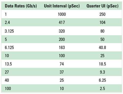
Review: When and why to care about glass-weave skew. At what frequency should you care? Each differential serial-channel standard and speed has its own tolerance for skew. Most standards or chip manufacturers offer guidance on skew tolerance, but we can generically characterize that a channel’s tolerance for skew is described as roughly 25% of the bit stream’s unit interval (UI). For example, a 1Gbps (500MHz) signal would have a UI of 1000ps. Using 25% as a guideline, that represents a 250ps skew tolerance. That’s a wide window, and that’s why most engineers didn’t need to worry about GWS 20 or more years ago.
Fast forward to designing at 10Gbps (5GHz). The unit interval is 100ps, and the skew tolerance decreases proportionally to around 25ps. PCI Express 4.0’s signaling speed, at twice the speed of PCIe-3.0, is even faster: at 16Gbps (8GHz). This maps to roughly a 60ps UI and 15ps of skew tolerance – half of the 30ps skew tolerance in PCIe-3.0.
TABLE 11 shows data rates (Gbps), unit intervals (ps), and approximate tolerances for skew (quarter UIs). If you aren’t dealing with GWS on your current designs, it’s likely you will in the not-too-distant future as speeds escalate.
Basic theory behind these alternatives. The underlying mechanisms by which the two GWS mitigation approaches in this column operate are actually very different.
Dual-ply glass seeks to reduce the probability that one signal in a high-speed differential pair will see systematic resin gaps because the two plies of glass have little likelihood of aligning identically under one another. This is illustrated in FIGURE 1. The blue top ply would, as a single ply, have resin-only “windows” (my term for it) similar to the larger yellow square shown in the figure. The red second ply of glass in the figure, including random manufacturing variation from panel to panel of glass, will typically serve to shrink the resin-only window, mitigating glass-weave-induced skew.
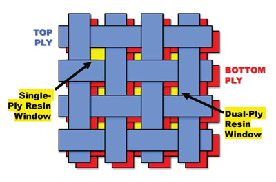
Low-Dk glass seeks to reduce the Dk variation a signal would see as it traverses the yellow resin windows shown in Figure 1. As discussed in Part One, standard E-glass has a Dk of around 6.8, while resin systems typically have Dks approaching 3.0. (This varies from laminate to laminate.) Low-Dk glass – typically manufactured by AGY in the US (L glass) or Nittobo (NE glass) in Japan – seeks to bring the glass Dk closer to the resin Dk, with typical values of 4.8, cutting the difference by roughly 50%. Since signal-propagation delay is proportional to the square root of the cross-sectional Dk, cutting the difference in half provides a significant benefit relative to mitigating glass-weave skew.
Electrical parameters for E-glass and low-Dk glass. I’ve done some research on Dk and Df (dissipation factor/loss tangent) comparisons between E-glass, L-glass (AGY, US), and NE glass (Nittobo, Japan), and concluded Dk and Df values for all but E-glass depend on whom you ask, when you ask, and of course frequency.
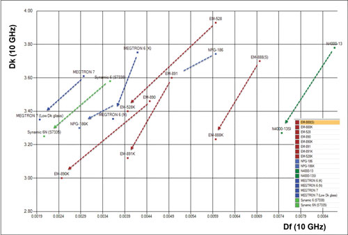
Park Electrochemical, now AGC-Nelco, was a pioneer in this space, launching N4000-13 with E-glass, and N4000-13SI with low-Dk glass, in 1996. In the words of Doug Leys, vice president of engineering at AGC-Nelco, “In 1996, achieving lower Dk was the primary concern, so the addition of low-Dk glass was a natural fit. Today, the driving force is reduced loss. Anything that can squeeze a little more attenuation out of the design is desirable.” Lower Dk values enable thinner dielectrics and thinner high-layer-count PCB stackups. Today, many laminates with low-Dk glass are on the market. FIGURE 2 shows a handful of materials from the Z-planner dielectric library that include both an E-glass version of the laminate, as well as a low-Dk glass version, using glass from either AGY, Asahi (a weaver rather than a supplier of yarn), or Nittobo. The vertical axis is Dk, and the horizontal is Df, both at 10GHz and 50% resin content. Arrows connect the E-glass laminates to the low-Dk laminates. Although we refer to this class of glass as “low Dk,” it’s clear from the figure that each of these products – and the underlying glass constructions – also offer much lower loss. Many more laminates are offered with low-Dk glass. Each laminate vendor uses its own convention for low-Dk glass. AGC-Nelco uses “SI” as a suffix. EMC, Nanya and Panasonic use “K.” Shengyi uses “N,” TUC uses “SP,” etc. Check with your fabricator for availability.
Availability and Cost Considerations
Availability. It should come as no surprise a fabricator may or may not have dual-ply core configurations in stock in the thicknesses you need. It’s even less likely it will stock low-Dk glass configurations unless it’s coordinated proactively. This is an important consideration, in fact. By comparison, other GWS strategies, like angled routing, artwork rotation, or routing differential pairs with the glass pitch, are all immediately available.
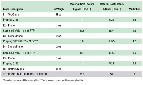
Cost. From a cost standpoint, it’s helpful to first realize the approximate cost breakdown for laminates. Roughly speaking, 50% of the cost of a core comes from the copper. Another 25% comes from the glass, and the final 25% comes from the resin (more or less, depending on the copper weight, roughness, glass type, and resin system). Obviously, for prepregs, it’s a 50:50 split between the resin and glass, depending on the resin system, resin content (%), and relative weight of the glass style. Using the above as a baseline, dual-ply glass does add additional cost, but for the same overall laminate thickness, the cost difference should be less than 10%.
Low-Dk glass, on the other hand, carries an additional cost of 50% for cores and roughly a 5x cost increase for prepregs (more or less, depending on the laminate vendor, PCB fabricator, and the day). Depending on the stackup, my history says this doubles the cost as a rule-of-thumb.
TABLE 2 shows a simple stackup comparing E-glass to L-glass cost factors. Note cores cost a good bit more than prepregs because of the copper. Designers should check with fabricators for specific pricing and lead times if they’ve reached the tipping point on speed and feel the need to incorporate low-Dk glass.
Glass-weave skew research. There isn’t a huge body of research to point to relative to glass-weave skew. The reason, in part, is the stochastic nature of the phenomenon. That’s not a word we use much in PCB design, but it definitely applies here. In other words, glass-weave skew has a random probability distribution that may be analyzed statistically but may not be predicted precisely. Anyone who’s taken an applied statistics class (for research purposes) knows getting good answers for something with a probability distribution requires a lot of data. In this case, a lot of comparative data require a lot of test structures with different glass configurations, trace orientations relative to the weave, and a lot of time in the lab. These are some of the issues we ran into when we embarked on an ambitious research project a few years ago.
With the support of laminate materials provided by Nanya Plastics, 66 different test vehicle configurations were fabricated, each with 160 nets: 40 parallel to the warp, 40 parallel to the fill, and 80 traces angulated to the warp or fill. As we expected, the 80 angulated traces showed the lowest line-to-line delay differences in the study. As mentioned in Part Two of this series, angled routing is a commonly-recommended design strategy for GWS control, and an approach that our research confirmed to be a reliable means toward preventing the problem. We sought to compare 13 different glass configurations outlined in FIGURE 3, including spread glass, non-spread glass, single-ply and dual-ply glass, along with standard E-glass (electrical-grade fiberglass) and low-Dk glass.
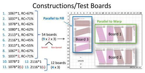
Test vehicles included eight different single-ply E-glass configurations, one single-ply L-glass configuration, and four different dual-ply glass configurations, including one using AGY L-glass. It was an ambitious experiment, and we learned with time that the scope of analyzing all the configurations was beyond our budget and time window. Nevertheless, we learned some interesting things I’ll share here.
First, we wrestled with the fact that tracking all the glass and “grain” (warp) direction details through the supply chain to finished boards was quite difficult. (You’re only as good as the weakest link in the supply chain as far as managing the details.) It’s important to consider this when negotiating changes in your design approach. Aligning GWS strategies with your fabricators is critical for any approach to be effective.
Second, we found about 75% of the time the weave wandered under our transmission lines enough to make it impossible to make firm statements about the skew results from the underlying constructions. The remaining 25% of the transmission lines provided a sample from which we could make some high-level determinations, although without being able to claim statistical significance based on the sample size. The variation, in terms of the weave orientation, was +/-5°, centered around 0° (perfect alignment).
Third, we learned an angle of only 0.5° was necessary between the glass and trace alignment to reduce glass-weave skew significantly – an unintentional, but interesting artifact.
Fourth, we confirmed that test traces routed at 15° relative to the glass weave predictably reduced skew to essentially zero. (In fact, our study showed that 7.5° would have done the job.)
Finally, we learned a few things that could be used as guidelines for further research. We learned that dual-ply glass, where we had the ability to make apples-to-apples skew comparisons, reduced skew significantly. Low-Dk glass did the same thing, and using these two factors in concert had the lowest skew in the study, excluding 15° angled routing.
Conclusion
Some mitigation techniques outlined in this four-part series are what I call “deterministic” solutions. These solutions, including artwork rotation and angled routing, are almost guaranteed to mitigate skew. In the case of angled routing, another benefit is the routing process is entirely within the OEM hardware team’s control, and – at the cost of board space – the practice only directly affects the high-speed differential interconnects about which you’re concerned.
Other mitigation techniques are “probabilistic,” meaning they reduce the probability of a skew problem, while not necessarily guaranteeing skew problems will never occur on a unit in high-volume production. See Part Two in this series for some of the skew-control techniques, roughly ranked in ascending order of cost in manufacturing. I’d be interested in your comments if this series rang true. Feel free to download the evaluation software that includes a tutorial for mitigating glass-weave skew from z-zero.com.
References
1. Lee Ritchey, Minimizing Skew in High Speed Differential Links, (video), 2015.
Bibliography
1. Scott McMorrow, et al, “Impact of PCB Laminate Weave on Electrical Performance,” DesignCon, January 2005.
2. Lee Ritchey, “A Way to Address the Problem of Jitter and Skew in Gigabit and Faster Signals Caused by Laminate Weaves,” Current Source, June 2007.
3. Eric Bogatin, “Skewering Skew – Laminate Weave Induces Skew,” Printed Circuit Design, April 2005.
4. Jeff Loyer, et al, “Fiber Weave Effect: Practical Impact, Analysis and Mitigating Strategies,” DesignCon, January 2007.
5. Eric Bogatin, Bill Hargin, et al, “New Characterization Technique for Glass-Weave Skew,” DesignCon, January 2016 and 2017.
